Features for the AM3358
| Parameter | Feature Description |
|---|---|
| Processor | High-performance 32-bit CPU (TMS320C28x) running at 150 MHz (6.67-ns cycle time) |
| Power | Low-power design: 1.8V core at 135 MHz, 1.9V core at 150 MHz, 3.3V I/O |
| JTAG | JTAG boundary scan support (IEEE 1149.1-1990) |
| MAC Operations | 16 × 16 and 32 × 32 MAC operations, including 16 × 16 dual MAC |
| Bus Architecture | Harvard bus architecture for parallel instruction/data processing |
| Memory | Up to 128K × 16 flash, 1K × 16 OTP ROM, 4M linear program/data address reach |
| On-Chip Memory | Multiple SARAM blocks: L0/L1 (2×4K×16), H0 (8K×16), M0/M1 (2×1K×16) |
| Peripheral Interrupts | Peripheral Interrupt Expansion (PIE) block supporting up to 45 interrupts |
| Motor Control | Two Event Managers (EVA, EVB), compatible with 240xA devices |
| ADC | 12-bit ADC with 16 channels, fast conversion rate of 80 ns/12.5 MSPS |
| Serial Ports | SPI, Two SCIs (UART), eCAN, McBSP for serial communication |
| GPIO | Up to 56 General-Purpose I/O (GPIO) pins |
| Emulation & Debugging | Real-time debugging via hardware, analysis and breakpoint functions |
| Development Tools | Code Composer Studio™ IDE, ANSI C/C++ compiler, DSP/BIOS™ |
| Power Modes | Supports IDLE, STANDBY, HALT modes for power savings |
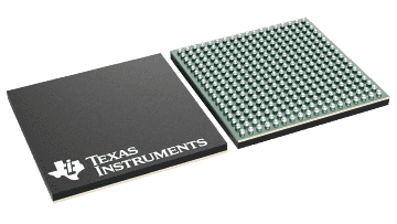
| Package Options | 179-ball MicroStar BGA™, 176-pin LQFP, 128-pin LQFP |
| Temperature Range | A: –40°C to 85°C, S/Q: –40°C to 125°C (AEC-Q100 for automotive) |
Description for the AM3358
The AM335x microprocessors, based on the ARM Cortex-A8 processor,
are enhanced with image, graphics processing, peripherals and industrial interface options such as EtherCAT and PROFIBUS.
The devices support high-level operating systems (HLOS). Processor SDK Linux® and TI-RTOS are available free of charge from TI.
The AM335x microprocessor contains the subsystems shown in the Functional Block Diagram and a brief description of each follows:
The contains the subsystems shown in the Functional Block Diagram and a brief description of each follows:
The microprocessor unit (MPU) subsystem is based on the ARM Cortex-A8 processor and the PowerVR SGX™ Graphics Accelerator
subsystem provides 3D graphics acceleration to support display and gaming effects.The PRU-ICSS is separate from the ARM core,
allowing independent operation and clocking for greater efficiency and flexibility. The PRU-ICSS enables additional peripheral interfaces
and real-time protocols such as EtherCAT, PROFINET, EtherNet/IP, PROFIBUS, Ethernet Powerlink, Sercos, and others.
Additionally, the programmable nature of the PRU-ICSS, along with its access to pins, events and all system-on-chip (SoC) resources,
provides flexibility in implementing fast, real-time responses, specialized data handling operations, custom peripheral interfaces, and in offloading tasks from the other processor cores of SoC.


